Logic levels
Section titled “Logic levels”Ranges of voltages are abstracted away into 0 (LOW) and 1 (HIGH).
The ranges have a gap in-between, to avoid errors by fluctuations.
Example: CMOS (LV)
- HIGH - 2V to 3.3V
- LOW - 0V to 0.8V
Digital waveforms
Section titled “Digital waveforms”Voltage levels that are changing back and forth between the digital states.
A sudden change between the digital states that lasts for a specific duration before returning to the original state.
2 types:
- Positive-going pulse: Sudden change from LOW to HIGH to LOW.
- Negative-going pulse: Sudden change from HIGH to LOW to HIGH.
Non-ideal pulse
Section titled “Non-ideal pulse”Even though analog signal is abstracted into digital, the analog characteristic can be observed when switching states. A non-ideal pulse will take a very short time to switch the states.
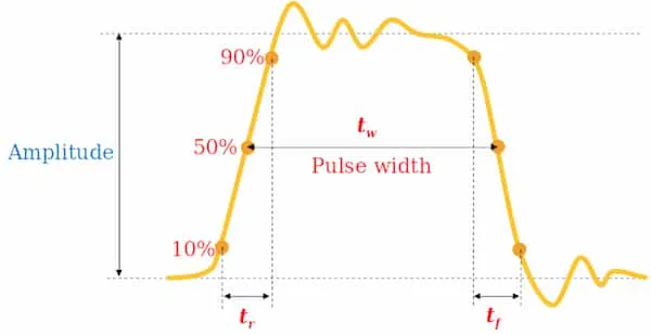
Raise and fall time
Section titled “Raise and fall time”Ideally a pulse is instantaneous. In non-ideal case, it takes time to transition between states. Raise and fall times are measured between the 10% and 90% transitions.
Pulse width
Section titled “Pulse width”The time a pulse takes. In non-ideal case, the pulse width is said to be the time between 50% marks of the transition.
Waveforms
Section titled “Waveforms”A series of pulses. They can either be periodic (pulse train) or non-periodic. A clock is required along with the waveform to convert it into binary.
Duty cycle
Section titled “Duty cycle”Defined for a periodic waveform. Ratio between pulse width () and the period ().
Gate delay
Section titled “Gate delay”Aka. propogation delay. The time it takes for a logic gate to produce an output after receiving an input. Caused due to the physical limitations of the gate’s internal circuitry. Denoted by .
Can vary betwen LOW to HIGH () and HIGH to LOW ().
Logic family
Section titled “Logic family”A collection of different integrated circuit (IC) chips/chip building blocks that have:
- Similar input, output and internal circuit characteristics
- Methods to implement all necessary logic functions
Chips from the same family can be interconnected to perform any desired logic function.
Chips from different logic families may or may not be compatible. When they aren’t, special steps must be taken to interconnect those chips/building blocks.
Electrical behavior
Section titled “Electrical behavior”- Logic voltage level
- DC noise margins
HighestLOWvoltage of an output must be always lower than the highest voltage that an output can reliably interpret asLOW - Fan-out
Maximum number of inputs that a single output pin can be connected to. - Fan-in
Number of inputs that a single component can support. - Power consumption
- Speed
- Noise/interference
- Electrostatic discharge
- Three-state outputs
Examples
Section titled “Examples”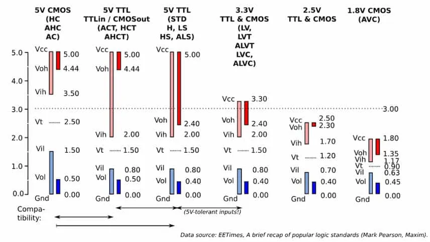
Image by Wired && Coded;
- Light colored strips are for input
- Dark colored strips are for output
- is the minimal voltage of output HIGH
- is the maximal voltage of output LOW
- is the minimal voltage of input HIGH
- is the maximal voltage of input LOW.
- Two gates of voltage standards (1) and (2) are compatible in the 1->2 direction if (1) > (2) and (1) < (2).
Digital Design
Section titled “Digital Design”Digital circuits are designed using software. Simulations are ran at logic level. Then the circuit is built using FGPAs. After many verifications, the circuit is fabricated as a chip.
Data transfer
Section titled “Data transfer”Data can be transferred in either serial or parallel. Serial transfer takes more time while parallel transfer requires more transmission lines.